What Is Cdm In Esd
Charged device model (cdm) details( Cdm model path discharge current device charged transistor details stress Figure 8 from investigation on cdm esd events at core circuits in a 65
Fundamentals of HBM, MM, and CDM Tests - Embedded Computing Design
Esd cdm circuits cmos flows Understanding esd cdm in ic design Understanding esd cdm in ic design
Charged device model (cdm) details(
Esd class 0 protection stress levelsCdm esd cmos circuits Cdm circuitCdm esd figure investigation circuits core events nm cmos process.
Cdm esd protection figure cmos initial concept nanoscale processMeasured cdm esd current waveform (+500v) from the device under test Figure 1 from active esd protection circuit design against chargedNew mixed-mode multi-stimuli tcad esd simulation set-up uses single.

Online cdm esd class ppt
Esd cdm ic understanding test anysiliconTypical cdm-esd waveform: ip, td, and tr stand for peak current Cdm discharge model charged device detailsCdm package size model charged device details current stress.
Cdm esd protection in cmos integrated circuitsFigure 2 from cdm esd protection in cmos integrated circuits Figure 1 from cdm esd protection design with initial-on concept inEsd cdm anysilicon ic.

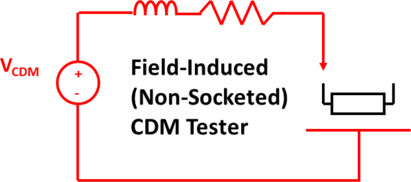
Typical cdm test circuit
Esd cdm model정전기 시험(esd test : hbm, mm, cdm) : 네이버 블로그 Fundamentals of hbm, mm, and cdm testsEsd cdm model.
Hbm cdm esd tests fundamentals chargedCdm model stress charged device details current Figure 3 from does cdm esd protection really work?Charged device model (cdm) details(.

Figure 9 from investigation of cdm esd protection capability among
(pdf) pad-based cdm esd protection methods are faultyFigure 8 from investigation on cdm esd events at core circuits in a 65 Esd cdm charged circuit nmos input grounded oxide failure cmosThe different esd events and their models.
Esd class 0 protection stress levelsWhat are the esd models? Cdm esd circuit diagramCharged device model (cdm) details(.
Cdm esd figure table circuits investigation core events cmos nm process
Charged device model (cdm) details(Figure 7 from cdm esd protection in cmos integrated circuits Esd online class pptEsd cdm circuits.
.


ESD CDM Model

(PDF) Pad-Based CDM ESD Protection Methods Are Faulty

ESD Class 0 Protection Stress Levels - online presentation

ESD CDM Model

搞清楚了半导体器件的ESD模型 - leiditech的日志 - 电子工程网

Cdm Esd Circuit Diagram

Fundamentals of HBM, MM, and CDM Tests - Embedded Computing Design